TechnologyPhotonic hardware

Memory made of light
AKME S1, the Akme Shadow One, is an integrated optical memory. Data is held as pulses of light in a silicon-carbide ring and read by an electronic chip bonded on top of it. Now in development, on its way to first silicon.

- Status
- In development
- Type
- Integrated optical memory
- Read-out
- 16-channel CMOS
- Stage
- Verified in simulation
Inside the chip
From the module to the light
One continuous descent, from the package to a pulse of light.
ModuleThe whole module
A black substrate with a machined frame, two chips and one optical port.
Two chipsOne stack
The photonic die holds the light. The read-out chip, bonded on top of it, reads it.
Sixteen channelsThe electrical side
Gold bond wires carry sixteen read channels from the die to the package.
The ringWhere the light is kept
A closed ring of silicon carbide, next to the guide that brings the light in.
The lightPulses in the ring
Pulses of light travel around the ring. Each pulse is a stored bit.
Inside the chip
From the module to the light
One continuous descent, from the package to a pulse of light.
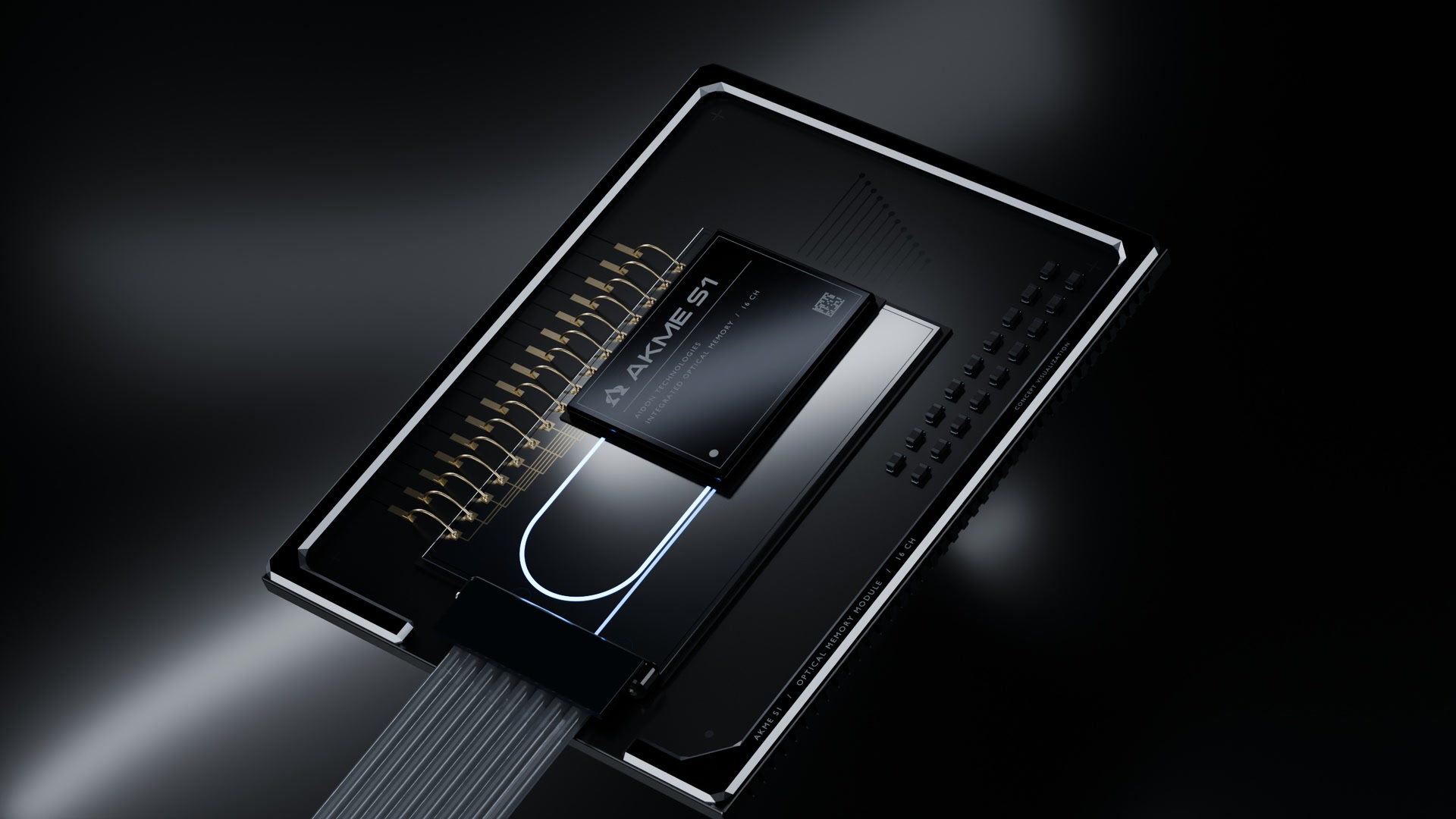
ModuleThe whole module
A black substrate with a machined frame, two chips and one optical port.
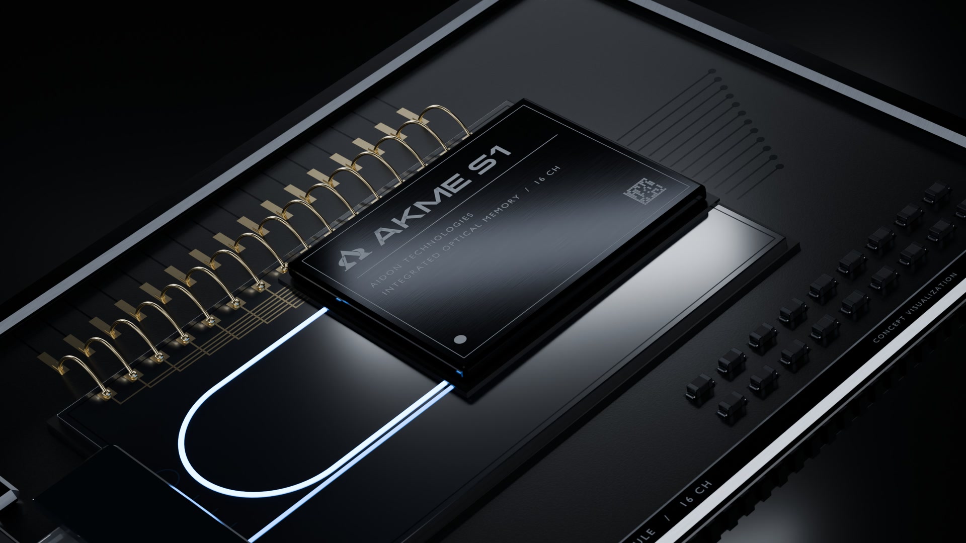
Two chipsOne stack
The photonic die holds the light. The read-out chip, bonded on top of it, reads it.
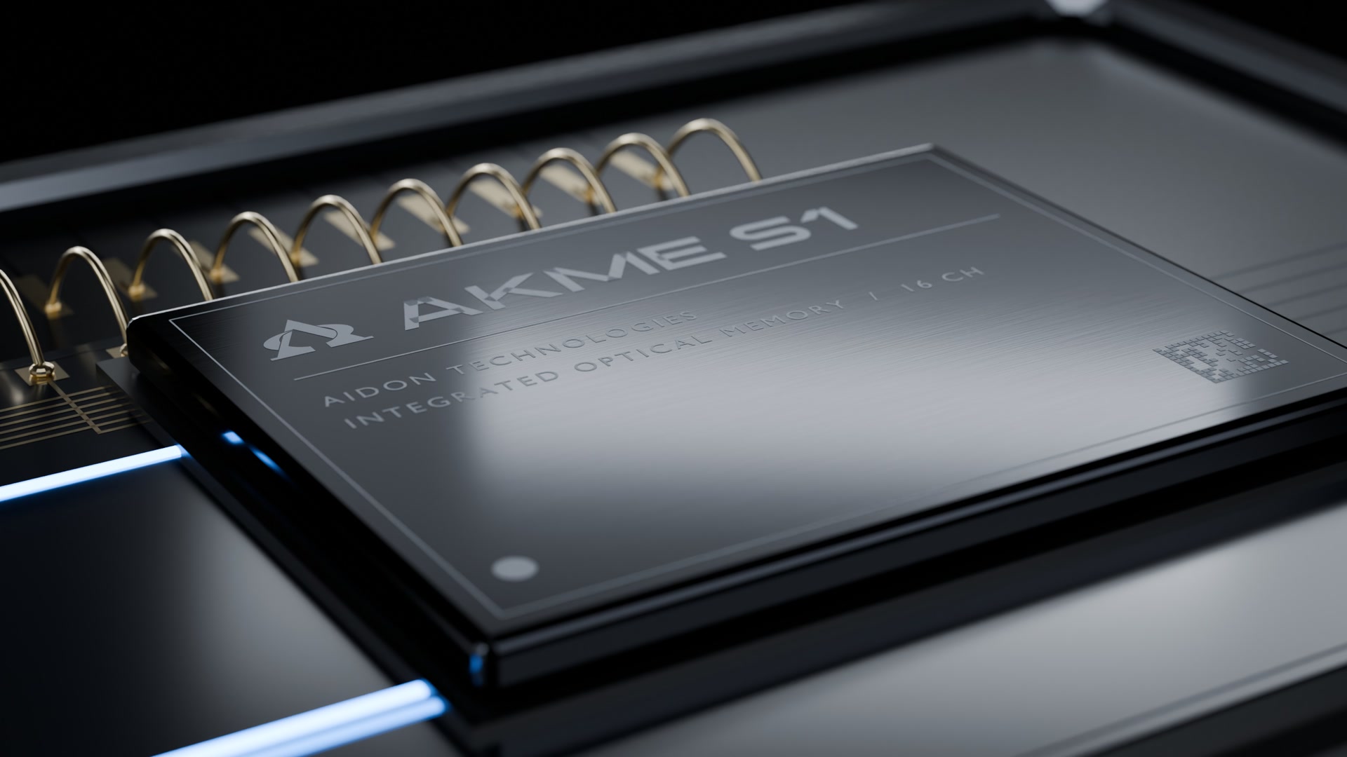
Sixteen channelsThe electrical side
Gold bond wires carry sixteen read channels from the die to the package.
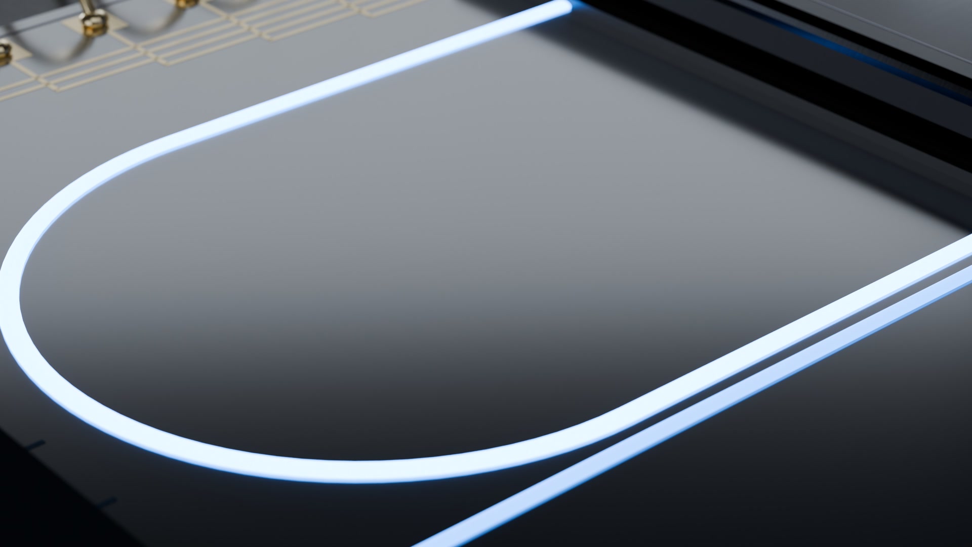
The ringWhere the light is kept
A closed ring of silicon carbide, next to the guide that brings the light in.

The lightPulses in the ring
Pulses of light travel around the ring. Each pulse is a stored bit.
Concept visualization
At a glance
read channels on the CMOS chip, built on an open 130 nm process.
digital block, closed across all 18 process corners with no violations.
optical receiver bandwidth, at 0.94 mW per channel.
reads through the full chain with zero errors.
Pre-silicon simulation and verification, before and after layout; full chain with an ideal converter. Not yet fabricated.
In plain words
Computers keep their data as electrical charge. This chip keeps it as light: tiny pulses that go round and round a ring, like runners on a track. A second chip on top watches the track and reads the pulses back as ordinary digital data.
For engineers
A silicon-carbide ring resonator holds optical pulses; a CMOS die on an open 130 nm process reads 16 channels. The digital block closes timing at 50 MHz across 18 process corners, the optical receiver reaches 3.30 GHz at 0.94 mW per channel, and the end-to-end read chain was simulated over 3.96 million reads with no errors, using an ideal converter.
Why it matters
We design the photonics, the electronics and the models that will use them side by side, and we verify the chip before any silicon is made. Owning the hardware under the models is what turns a method into a product.
Anatomy
How it is put together
Five parts, each with one job. The images above show a representative package, built to the same rules as real photonic assemblies. It is not the layout of the chip.
- Photonic dieA ring of silicon carbide and the waveguide that feeds it. Pulses of light circulate in the ring; each pulse is a stored bit.
- Read-out chipA 16-channel CMOS chip bonded on top of the photonic die. It turns light into digital data.
- Optical interfaceA fibre array meets one edge of the die. That whole edge is reserved for light.
- Electrical interfaceGold bond wires along the edge that runs parallel to the fibres, in a single row.
- PackageA black substrate with a machined stiffener frame, open on the optical side.
Roadmap
From design to first silicon
Design
Light as memory
A ring of silicon carbide keeps pulses of light circulating. Each pulse is a stored bit. A 16-channel CMOS chip sits on top and reads them.
Closed in simulation
Verified before silicon
The photonic layout is frozen. The digital block closes timing at 50 MHz in every process corner, the receiver reaches 3.30 GHz, and the full read chain ran 3.96 million reads without an error.
Next
Towards first silicon
The fabrication package and the characterisation of the first chips. Until then, every statement here is a result of design and simulation.
Contact
Talk to the founders
Get in touch. We would be glad to share our ideas and walk you through the results, the proof and the measurements.